
Key Points:
- For metasurface fabrication, material selection relative to the wavelength is critical both for device performance and nanofabrication feasibility
- Different lithography tools offer various advantages and disadvantages in terms of achievable feature size and throughput. Processes that work well for prototyping are often not possible to scale to high-volume production
- Designers should be aware of constraints and opportunities with different nanofabrication processes in order to ensure their designs are within tolerances and compatible with existing processes
Overview
Fabrication of metasurfaces is a critical step in the sequence of designing and building meta-optical systems. While we can design and simulate more or less whatever we want (within the computational limits of FDTD and analogous methods), fabrication has far more stringent limits. The exact process will depend on the selected material(s) and design wavelength, critical dimensions and aspect ratio, required tolerances, available equipment, and fabrication budget. In this article, we’ll describe some of the key considerations of the fabrication process that a designer should keep in mind to ensure their device meets the performance requirements of their application. We’ll also provide an introductory overview of some of the key tools and process steps used by process engineers for making meta-optics.
This article focuses primarily on materials, aspect ratio, and some tooling considerations. A future post will touch in more detail on performance implications of different fabrication imperfections (e.g., point-like defects, overetching, underetching, sidewall angle, etc.).
Materials and Design Wavelength
Material selection has major implications for both device performance and fabrication feasibility. Typically, higher refractive index materials will enable higher diffraction efficiencies and are often preferred by a designer; however, depending on the design wavelength, this can come with a higher extinction coefficient as well. Standard materials for metasurfaces include crystalline and amorphous silicon, silicon nitride, titanium dioxide, gallium nitride, and niobium pentoxide. Refractive indices for these materials range from around n = 2.0 up to about n = 3.5, providing a wide range of options to designers. Some of these materials are far easier to work with, however, and have already existing processes at a number of foundries.
For example, silicon and silicon nitride are very standard materials with established deposition and etch processes, with well-studied chemistries and entire industries and supply chains built around working these materials. While developing processes with such materials is not necessarily trivial, they offer a great degree of flexibility in process tuning and options for equipment and fabs to work with.
Silicon becomes heavily absorptive in the visible range, limiting its utility primarily to the telecom range and longer wavelengths—some recent works have demonstrated its potential for visible range operation with ultrathin silicon films, but there are still notable efficiency losses at the blue side of the visible spectrum. Silicon nitride instead offers a much wider bandgap and is transparent across the full visible range into the ultraviolet. A major downside of silicon nitride is that it has a much lower refractive index compared to that of silicon, closer to n = 2.0, which usually limits the diffraction efficiency. Process engineers can mitigate this by adjusting the silicon content in the silicon nitride layer, sometimes leading to silicon nitride with higher indices, though this often comes with absorption losses.
Titanium dioxide is a promising material for metasurfaces as it exhibits a relatively high index closer to n = 2.4, depending on the formulation, while offering transparency across the visible and near-infrared (NIR) range. Titanium dioxide is unfortunately a challenging material to process. There are often a number of challenges in depositing thick films of the material while maintaining uniformity. A common deposition method used in metasurface fabrication based on titanium dioxide is atomic layer deposition (ALD). While such processes have led to a number of seminal research results in the metasurface community, processes based on atomic layer deposition into patterned resist films followed by back etching can also lead to voids within pillars. These can be mitigated through adjustments to the resist profile and ALD parameters, but ALD processes are also notoriously slow, often requiring 10 or more hours for a deposition. As such, ALD applied in this manner usually can only be justified when large batches of wafers are processed simultaneously, requiring large volumes to justify the cost and time.
Other materials such as niobium pentoxide, gallium nitride, and even indium tin oxide (ITO) show promise as metasurface materials, as they exhibit transparency in the visible range and relatively high refractive indices. Prototype metasurfaces based on these materials have been developed and are reported in the literature. There is potential for even engineering polymer-based metasurfaces wherein suspended nanoparticles (e.g., based on titanium dioxide) enable engineering of the refractive index based on the nanoparticle concentration. This would facilitate print-like processes for building metasurfaces without requiring any etching. Alternative direct printing methods with all-inorganic materials exploit nanoparticle composites based on ALD onto nanoimprinted films, enabling refractive indices in the 2.0 to 2.5 range.
Such processes are still in development but potentially offer substantial benefits in reducing the number of process steps to prototype a design, and enabling designers to tailor the refractive index requirements for the given application.
Example Process Flow
A typical metasurface process flow will start with a bare substrate (e.g., silicon or fused silica, depending on the operating wavelength). The device layer that will ultimately be patterned to form the scatterers is then deposited, typically via plasma-enhanced chemical vapor deposition. The thickness of this film will depend on the target wavelength and refractive index, but it is typically on the order of one wavelength thick (e.g., in the visible range with silicon nitride, this is often close to 600 nm). Once this film is deposited, there are a few options for how to progress, depending on whether you need a hard mask or if a resist will provide sufficient selectivity to etch through the device layer. Ultimately, however, there will be a lithography step. In an academic context, this will often require an electron-beam lithography system or high-resolution direct-write tool (if working with longer wavelengths in the mid-wave or long-wave infrared)—more high-throughput options are available at foundries.
If the resist is high selectivity, then you can proceed directly to etching the device layer. If a hard mask is required, there is an initial patterning step in which the hard mask is etched or formed via lift off. Ultimately, the device layer will be etched, usually via an inductively coupled plasma etch process. The etch mask or resist layer is then removed via immersion in a solvent bath and the wafer can proceed to subsequent steps including metrology and dicing.
We described the broad strokes of a metasurface process here, but the details can vary significantly depending on the tools available and materials being used. Other key steps including substrate cleaning with oxygen plasma, additional lithography and patterning steps to define any necessary aperture layers or other fiducials to facilitate integration of diced components with other elements, adhesion promotion prior to lithography, and intermediate metrology steps to evaluate each key process step. Additional details with sample process parameters can be found in some of the references at the end of this post.
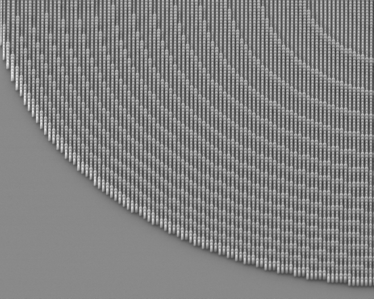
Critical Dimensions and Aspect Ratio
Of central importance to device performance as well as process optimization are the target specifications and their tolerances. These will largely dictate the types of tools and required processing for a metasurface. The critical dimensions include both the smallest feature as well as the smallest gap, which are for the most part dependent on what lithography tool is used, but it will also depend heavily on subsequent etch steps that alter features first defined in the resist layer.
Of crucial importance is the aspect ratio, referring to the height of the pillars scaled by the smallest feature size. It’s not uncommon to need aspect ratios of 5:1 or 7:1 in metasurface designs, but designers often would prefer 10:1 or better. In practice, it’s difficult to reliably achieve aspect ratios of 10:1 or higher with high yield, as many nanostructures tend to collapse due to lateral etching at that point as sidewalls are not perfectly vertical. In the visible range, to achieve full 2pi phase coverage, it’s typically necessary to have features on the order of 100 nm, though being below this for both minimum feature and minimum gap is often necessary to maximize device performance.
Feature size requirements are more relaxed for longer wavelengths in the NIR and beyond, though film thickness increase in proportion to the wavelength, thus often maintaining comparable aspect ratio requirements.
Equipment and Budget
One of the most important selections of equipment in a metasurface nanofabrication process is the lithography tool. This will largely drive both costs and throughput. At one extreme is electron-beam lithography. This is perhaps the most flexible tool, capable of achieving feature sizes on the order of 10’s of nm, but this is very low throughput and is really only practical for very small volumes, early-stage prototyping, or research purposes as the write times are long and cost prohibitive. There are a wide range of different photolithography tools available, including direct-write tools (i.e., equivalent to electron-beam lithography but with an optical beam, achieving coarser features and faster write times), contact lithography, immersion lithography, and projection-based systems.
Direct-write tools again are best suited for small volumes because of their limited throughput, and contact lithography tends to have fairly coarse features. Projection-based systems (e.g., standard DUV stepper lithography) can achieve features closer to 200 nm and as such tend to be limited to longer wavelengths, whereas immersion stepper lithography offers competitive feature sizes.
Extreme ultra-violet (EUV) systems offer state-of-the-art resolution on the order of 10’s nanometers, but this equipment is usually beyond the needs of what a metasurface would require, and foundries would be unlikely to displace other processes on their line to support metasurface fabrication unless there was a very large established market, as anyone attempting to make a metasurface with such equipment would be competing with semiconductor companies with a very strong business case for using tool time.
Another option is to use nanoimprint lithography. This approach essentially uses a master pattern, or stamp derived from a master, that is physically imprinted into a resist profile to define the necessary features. The master itself is usually generated via electron-beam lithography and can be quite costly; however, when many copies of a pattern are generated this cost is amortized across each device. Nanoimprint offers the capability to pattern large wafer areas with fine features (i.e., 100 nm or less).
Summary
There are a number of key considerations for designers when evaluating and determining how to fabricate their design. The fabrication requirements will ultimately impose constraints on the design, often requiring an iterative process between the two in order to maximize performance. Material selection relative to the design wavelength is important to balance efficiency as well as fabrication ease. Critical dimension and aspect ratio are two critical parameters for both design and fabrication and are often difficult to extend beyond 7:1 with high yield in practice, though it is possible with process optimizations. A number of different lithography tools and process flows exist for building metasurface components. The exact process for any design will largely be driven by cost and throughput considerations, and what may make sense for prototyping is unlikely to be a cost-efficient solution for high-volume production.
Additional References
Khorasaninejad, Mohammadreza, et al. “Metalenses at visible wavelengths: Diffraction-limited focusing and subwavelength resolution imaging.” Science 352.6290 (2016): 1190-1194.
Yang, Jianji, and Jonathan A. Fan. “Analysis of material selection on dielectric metasurface performance.” Optics express 25.20 (2017): 23899-23909.
Bayati, Elyas, et al. “Role of refractive index in metalens performance.” Applied optics 58.6 (2019): 1460-1466.
Einck, Vincent J., et al. “Scalable nanoimprint lithography process for manufacturing visible metasurfaces composed of high aspect ratio TiO2 meta-atoms.” ACS Photonics 8.8 (2021): 2400-2409.
Colburn, Shane, Alan Zhan, and Arka Majumdar. “Varifocal zoom imaging with large area focal length adjustable metalenses.” Optica 5.7 (2018): 825-831.
Colburn, Shane, et al. “Broadband transparent and CMOS-compatible flat optics with silicon nitride metasurfaces.” Optical Materials Express 8.8 (2018): 2330-2344.