
Key Points:
- Meta-atom design is an iterative process that requires balancing optical performance, fabrication constraints, and system-level goals from the start. While many research papers report on various meta-atom designs, there are a number of design details and tricks of the trade that are usually omitted
- Material choice, geometry, and feature complexity all introduce tradeoffs in efficiency, tolerance to fabrication errors, and manufacturability. In some cases, periodic meta-atom designs that are inferior in theory (i.e., reduced phase coverage and coarser feature sizes) are higher performing in spatially-varying meta-optics in practice owing both to fundamental reasons (e.g., from off-axis nulls in meta-atom scattering profiles) and reduced sensitivity to fabrication errors
- Complex meta-atoms bring real performance advantages, but realistic fabrication defects can limit yield and as-fabricated performance. If sufficient for your use case, simpler but well-validated designs paired with dedicated test structures in your design layouts often lead to more reliable results and fewer process iterations than relying on more aggressively optimized or overly complex meta-atoms
Overview
Designing meta-atoms for a given application is often an iterative process and can take on many forms depending on your use case, manufacturing constraints, and computational resources. While there is extensive literature and research papers detailing existing meta-atom designs, it’s rare that the practical details and tradeoffs encountered during the meta-atom design process are documented and made publicly available.
In this post, we aim to walk readers through some of the key considerations and tradeoffs that one may encounter, focusing on intuition rather than any single specific numerical design example, including from selecting materials and geometries, to designing your nanofabrication layouts to incorporate test patterns that will provide useful information for troubleshooting performance issues with fabricated devices.
Before You Simulate Anything, Clarify Your Design Goals and Constraints First
When presented with a research problem or a set of customer specifications, as engineers and scientists, it’s not uncommon for us to immediately jump into the design process, testing parameters and configurations to get a feel for the problem at hand. This can be fine, but it’s best to keep this brief until you ensure you have a firm understanding of the designs goals and constraints.
Initial feasibility studies are quite useful for gaining some quick intuition, but go back to your customer, manager, PhD adviser, or whoever it was that put you to the task of this design problem in the first place. Talk to them and obtain a more holistic understanding of the problem before you go much further. It often will save you design time, reduce the number of process iterations required, and get you closer to what you/your customer actually need, rather than what you think is needed upfront. A few lines of questioning that are usually informative include the following:
- Are there restrictions on feature size, aspect ratio, or materials for your customer/research problem?
- Do you understand enough about the end goals, downstream of the meta-atom design that may subsequently force your hand into a particular geometry, material stack, or other configuration because there is a specific efficiency threshold needed?
- Or is cost more important than optical performance, which would justify using coarser features and more standard materials that will reduce efficiency but may substantially reduce manufacturing costs?
- Are certain feature shapes more feasible with the intended nanofabrication process (e.g., rounded features rather than sharp edges), even if the sharp-edged designs could provide better performance in simulation?
This all may sound quite obvious, but it comes up in practice very frequently. We harp on this as it’s extremely common for weeks or months of development time to be used up, utilizing a design that does not meet the requirements of the problem at hand, because assumptions were made upfront that could have been avoided by taking a step back and thoroughly understanding the problem at hand first.
This is common especially for students or newcomers to meta-optics, but it happens with seasoned experts as well that operate with the same working assumptions that they’ve used on other projects. If you can avoid it, don’t make assumptions and ask for clarification instead.
Select a Material That Balances Optical Performance and Process Feasibility
Once your goals and constraints are better clarified, you need to select your substrate and meta-atom materials. Meta-atom material selection is one of the most consequential decisions for your design, both for optical performance and the implications for manufacturing. For the most part, a higher index material will provide better performance in terms of diffraction efficiency and stray light. At lower refractive indices, diffraction efficiency reduces, and this is exacerbated as the numerical aperture or phase gradients in the corresponding phase mask increase. The exception to this is when your refractive index is high enough that the material’s extinction coefficient becomes nonzero, introducing efficiency losses from absorption rather than just diffraction efficiency losses. In some cases, transmission losses due to absorption are tolerable if it means your diffraction efficiency is enhanced.
Separate from optical performance, you need to balance manufacturing considerations for different materials. Some materials with high refractive index (e.g., titanium dioxide) are commonly used for metasurface meta-atoms in the visible range, but these materials are not always as straightforward or as cost effective to fabricate as lower index counterparts (e.g., silicon nitride). In some cases, these more expensive processes are justified, and in other cases they are not, dependent upon your target application and manufacturing path. As part of the material selection process, it’s often worth explicitly simulating amongst the options available and making a rigorous comparison of efficiencies and evaluating alignment with your process specifications/constraints.
Bear in mind that materials often have distinct process constraints (e.g., some materials exhibit greater nonuniformity of films relative to others, even with the same target thickness and deposition tool), and differences in etch chemistries to accommodate distinct meta-atom materials can alter the achievable sidewall angles and surface roughness even if the target feature shapes and dimensions are otherwise identical.
Don’t Blindly Optimize from the Outset, Start from a Reference Design or Literature Result as a Baseline (if one is available)
There is extensive literature out there documenting meta-atom designs for various materials, wavelength ranges, and feature shapes. Do you really need something custom, or is there already an existing solution that you can work from?
For IP reasons, it of course may be necessary to use something else, but for purely R&D/educational purposes, or if working with a foundry partner for manufacturing that can license their own process/design IP, then this is not always the case.
Even if you need something custom, to align to your own process rules or specific target wavelength, it’s still worth getting a baseline for comparison so that you can benchmark your design against an existing solution, or at the very least have a sanity check on the physical validity of your modeling. For simple meta-atom designs this is less critical, but this can become especially relevant for more complex meta-atoms with multiple scatterers per unit cell, or with inverse-designed topology-optimized unit cells that have permittivity distributions for which there is really no underlying intuition for their physical operation.
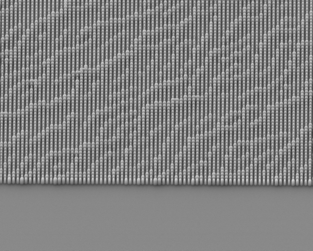
Taller Meta-atoms with a Wider Range of Feature Sizes Boost Phase Coverage but Increasing Phase Coverage Has Diminishing Returns (and sometimes reduces optical performance)
Meta-atom thickness is a critical parameter for optical performance and significantly affects process feasibility. In many cases, high aspect ratio nanostructures tend to provide better performance, enabling a wider range of phase delays that can be imparted with your meta-atom library. Typically, one will increase the thickness to the point where you are just within the aspect ratio limit of your process, thereby guaranteeing you can impart the largest phase shifts. This can present problems though. With a taller pillar, a small change in feature width induces a larger change in phase shift. Given tolerances on fabricated feature widths, this can mean larger phase error in your fabricated designs. This error may be small, but it should be accounted for.
Furthermore, simply achieving a wider range of phase shifts is not actually always better. With all else equal (i.e., same thickness, material, and period), meta-atom libraries with a more restricted phase range can actually provide enhanced efficiency because larger feature width nanoposts often exhibit modes arising from higher order resonances that have scattering profiles with off-axis nulls (Arbabi, 2020). Counterintuitively, this means that having a narrow range of feature sizes with a lower range of phase delays, even if below 2pi, can sometimes improve your efficiency.
Keep your Meta-atoms as Simple as Possible and Only Increase Meta-atom Complexity (e.g., asymmetric nanostructures, multiple elements per unit cell, multi-layer designs, topology-optimized designs, etc.) if it’s actually necessary for your application
Complex meta-atoms can bring a number of capability enhancements that with conventional optics often require multiple surfaces and components, including multiplexing across lightfield parameters (e.g., polarization, frequency, and wavevector), resonances that can be exploited for spectral filtering or enhanced light-matter interactions, bound states in the continuum, and other more exotic phenomena.
In these cases, more primitive meta-atom shapes often won’t provide the necessary performance. These types of complex meta-atoms that rely on resonant effects for their operation are inherently more sensitive to fabrication defects. As such, the required manufacturing processes require tighter tolerances. A designer will need to conduct tolerancing analyses to gauge the sensitivity to common fabrication defects (e.g., overetch, underetch, sidewall angle, surface roughness, feature width error, etc.).
Aside from some of the use cases just mentioned, where complexity in the meta-atom design is really needed (e.g., polarization multiplexing requires asymmetry in the scatterer design), designers should stick to primitive shapes with coarser features when it’s possible. It can be tempting to utilize topology-optimized metagratings, or other more advanced meta-atoms, as these designs can provide real performance advantages when there is a tight correspondence between the design and fabricated device. Under realistic fabrication constraints, however, these advantages are not often realizable in practice with high yield with high throughput tools. This is likely to improve with time with further investments in metasurface processes at foundries.
The point is to not overengineer your component, to design with fabrication constraints in mind, and to keep things as simple as possible for your use case (i.e., use primitive shapes when you can, and avoid fine and sharp features if your application doesn’t actually require those for optical performance reasons).
Check and Recheck Your Simulation Results
Once you have settled on a meta-atom library and have struck an acceptable balance between optical performance and process feasibility, make sure to validate your results. Simulations are great, but they are often flawed and based on crude assumptions that abstract out much of the underlying physics in the problem. We recommend conducting checks within the same simulation environment as well as cross validating with a distinct type of simulator.
For example, if you designed your meta-atom library with a finite-difference time-domain simulator, you’ll want to check the convergence behavior and verify that your phase and amplitude response vary minimally as you make adjustments to your mesh size, as you add additional perfectly matched layer (PML) stacks at the boundaries, and as you vary the spacings between your field monitors and devices.
If instead you designed your meta-atom with RCWA from the outset, you should adjust both the spatial discretization as well as the number of Fourier harmonics utilized in the simulation. With a low number of harmonics, the simulated permittivity profile for a meta-atom can often mismatch the desired profile substantially, but it can quickly converge as the number of orders used increases. You’ll want to confirm you are simulating within a converged number of orders.
If you simulate your meta-atoms with RCWA, it’s worth checking the result when simulated in FDTD and vice versa (or with another simulation methodology). In some cases it’s not possible or practical to simulate a particular meta-atom design with a given technique. For example, RCWA is usually a poor fit for metals or very high contrast materials, which may force a designer to use a different approach such as FDTD. In that case, it is often still worthwhile to verify results with an alternative formulation of a simulator (e.g., there are now many commercial and open-source options for FDTD simulation and these can be compared against one another).
This type of cross validation with multiple simulators unfortunately can be cost prohibitive for cash-strapped academic research groups or small businesses where a lot of meaningful innovation in the field occurs. At EdgeDyne, we are aiming to address this with a holistic metasurface SaaS simulation tool that is affordable for both academics and small businesses that have tighter budgets.
Ensure your design layouts will provide relevant experimental information when you have a fabricated sample
Once your meta-atom library is validated and you have confidence in your simulations, you can proceed to incorporating this into full component designs, mapping meta-atom geometries to positions in a layout to realize a target phase mask for your appication. When taping the design out into a layout file for fabrication, it’s worth including a number of test structures to facilitate data collection for troubleshooting. This includes making various test patterns and components that are standard across most of your layouts that allow you to characterize efficiencies for different feature ranges and deflection angles. Options for these include small aperture variants of beam deflectors with different deflection angles, metalenses over a range of target NAs, and uniform arrays of features swept over your meta-atom library feature range.
This is extra work to generate these patterns (though these can be largely automated as part of your design flow) and in some cases you may never actually test these patterns if your full component with your target phase mask performs well on its own. Incorporating these test structures is still good practice though. Why? If your component exhibits a phase profile corresponding to a freeform optic, or has a target point spread function that is more complex with multiple lobes or other advanced behavior, and if it does not function within specification on your first fabrication iteration, then these test patterns can provide valuable information for troubleshooting purposes.
Is the discrepancy between your component’s experimental performance and the simulation due to your meta-atom design itself or because of fabrication error that your models did not capture? How could you go about decoupling these if you only have your full component design but no additional test patterns that you can utilize to probe your meta-atoms under simpler design conditions?
Beam deflectors across various angles can be characterized in a straightforward manner, providing empirical efficiency data that can be compared across subsequent fabrication runs to monitor process stability and improvements. Arrays of uniform feature meta-atoms provide regions for inspection to measure realized feature widths, providing data on how biases may need to be modified in subsequent layouts to better dial in dimensions.
If you have space in your layout, add test structures along these lines or other patterns more relevant to your full component design. Think about how you’ll test your design and what the next steps will be if it doesn’t perform as intended. How may it fail and what data would you need to confirm that is indeed what is happening? This is really just sound experimental design, but it also can save you time (and money) by reducing process iterations.
Summary
In this article, we highlighted some of the practical considerations in meta-atom design. It’s critical to balance optical performance with fabrication feasibility and to maintain perspective on the end goals as you formulate your design problem. Material selection is a critical early choice in the design process and then the type of features that you use. Emphasizing simplicity in your meta-atom design tends to increase likelihood of success in terms of performance and yield. While there are many technical details of how you simulate meta-atoms, including the impact of thickness and feature ranges, most mistakes can be avoided through thorough understanding of your design and test constraints, and maintaining a degree of skepticism about simulation results throughout the design process.
References
Arbabi, Amir, et al. “Increasing efficiency of high numerical aperture metasurfaces using the grating averaging technique.” Scientific reports 10.1 (2020): 7124.
Zhan, Alan, et al. “Low-contrast dielectric metasurface optics.” ACS photonics 3.2 (2016): 209-214.
Yang, Jianji, and Jonathan A. Fan. “Analysis of material selection on dielectric metasurface performance.” Optics express 25.20 (2017): 23899-23909.
Bayati, Elyas, et al. “Role of refractive index in metalens performance.” Applied optics 58.6 (2019): 1460-1466.
Arbabi, Amir, et al. “Dielectric metasurfaces for complete control of phase and polarization with subwavelength spatial resolution and high transmission.” Nature nanotechnology 10.11 (2015): 937-943.