
Key Points
- At modest +1-order diffraction angles, a conventional multi-level diffractive optical element can perform very well. Performance in either platform depends strongly on whether the design properly accounts for sampling, material properties, fabrication limits, and the relevant electromagnetic effects, so comparisons should apply equivalent design rigor and constraints to both.
- The distinction is sometimes partly semantic and partly a consequence of different research communities. Once a multi-level DOE contains subwavelength features and must account for vector effects, coupling, and resonances, it can reasonably be viewed as a type of metasurface, even if it is described using traditional diffractive-optics terminology.
- Material selection affects the two platforms differently. In a scalar surface-relief optic, refractive index primarily changes the required relief depth and overall transmission. In a metasurface or full-wave subwavelength DOE, it also changes modal confinement, coupling, angular response, fabrication tolerance, and the available design space.
- At larger +1-order target diffraction angles, the required phase period becomes small, scalar assumptions begin to break down, and typical minimum-feature-size limits can prevent multi-level DOEs from adequately sampling the ideal phase profile. In this regime, a properly designed single-layer metasurface can remain highly efficient relative to conventional alternatives, while a competitive subwavelength DOE generally requires similar full-wave design methods as used for metasurfaces
Introduction
A recurring question in meta-optics is whether metasurfaces offer a meaningful advantage over conventional diffractive optical elements, or whether they are simply a more complicated way of implementing the same phase profile. The answer depends strongly on the operating regime.
At relatively low numerical aperture, or for modest beam-deflection angles, a conventional multi-level DOE can implement a spatial phase profile very efficiently. If the design does not require polarization control, wavelength multiplexing, angular selectivity, or another function that relies on the nanostructure itself, there may be little intrinsic optical reason to use a metasurface.
The situation changes as the required phase gradient increases. The physical distance over which a complete 0 to 2π phase ramp occurs becomes smaller, making the profile more difficult to sample within realistic manufacturing constraints. At approximately the same point, scalar diffraction theory becomes less accurate and electromagnetic interactions between neighboring structures become important. This is where metasurfaces can begin to offer a substantive advantage, particularly for large-angle beam steering.
We use beam deflectors as a representative example because more complex phase profiles can often be understood as spatially varying combinations of local deflection angles. A lens, for example, applies a progressively larger deflection angle as the radial distance from its center increases. The response of a complete optical element cannot always be inferred solely from isolated gratings, but this provides a physical reason to expect many of the same trends to remain relevant for lenses and other spatially varying phase profiles.
The comparison here is intentionally narrow. We consider conventional surface-relief diffractive optics and dielectric metasurfaces used primarily for spatial phase engineering. Additional metasurface capabilities, such as polarization multiplexing or simultaneous control of multiple light-field parameters, would make the comparison less direct. “Binary optics” is also used broadly here to include quantized, multi-level approximations to a blazed phase profile rather than only strictly two-level structures.
Similar Target Phase, Different Phase Shift Mechanism
For a conventional surface-relief optic, the phase delay is produced primarily by propagation through a spatially varying material thickness:

A complete 2π phase shift therefore requires a relief depth of approximately:

Changing the refractive index does not fundamentally alter this mechanism. A lower-index material requires a deeper profile, while a higher-index material requires a shallower one. Material selection still affects Fresnel reflection, absorption, etch depth, surface roughness, sidewall quality, and coating options, but to first order the normalized relief profile can be transferred between materials by adjusting its depth.
A dielectric metasurface operates differently (Figure 1). Instead of a staircase-like surface, it may contain an array of nanoposts with varying lateral dimensions. The response depends not only on optical path length, but also on modal confinement, reflections, coupling between neighboring structures, and angular scattering. Changing the refractive index therefore changes the available phase and amplitude response, the required geometry, and the interaction between adjacent elements.

This distinction is especially important when comparing silica with higher-index dielectric platforms. A silica DOE can produce a complete 2π phase delay simply by being made sufficiently deep. A simple silica nanopost metasurface may instead have weak modal confinement and a restricted design space, particularly for large-angle deflection.
This does not mean that silica metasurfaces cannot work well. It means that a single low-index nanopost grating design should not be treated as representative of what metasurfaces more generally can achieve.
What Constitutes a Fair Comparison?
Several studies have compared conventional diffractive optics and metasurfaces, with some concluding that metasurfaces provide little or no efficiency advantage. The objective is reasonable. Metasurfaces are sometimes presented as inherently superior, when in reality they still exhibit phase errors, reflection, absorption, unwanted diffraction orders, and stray light. These are real issues, but their impact depends strongly on the design, material platform, and operating conditions.
One published comparison used a low index nanopost platform for high NA metalensing and reported surface relief designs with an NA of 0.99. Based on the stated design period, however, our calculation suggests that the phase profile is substantially aliased and supports an unaliased NA closer to approximately 0.6. Under this interpretation, the results remain informative for the particular structures studied, but they do not provide a general indication of the performance limits of either platform.
Requiring both devices to use the same material does not necessarily create a fair constraint. A low-index material may be entirely adequate for a deep surface-relief optic while being a poor choice for a compact nanopost metasurface. Matching the material can therefore appear controlled while disproportionately limiting one side of the comparison.
A metasurface designed for one angle should also not be expected to remain optimal at every other angle. As the grating period changes, so do the arrangement of structures within the supercell, coupling between elements, and the supported modes. A design that works well at 10° may perform poorly at 40°, even though another design optimized specifically for 40° performs much better.
We interpret these discrepancies as differences in design assumptions and comparison methodology rather than evidence of a general limitation of metasurfaces. Regardless, a metasurface that performs poorly outside its intended design condition does not provide a strong basis for drawing broad conclusions. A useful comparison should optimize each structure for the target wavelength and angle, apply consistent efficiency definitions, use realistic materials and fabrication constraints, and distinguish conclusions about a specific geometry from conclusions about an entire class of devices.
Sweeping the Metasurface Design Space
To illustrate these effects, we can begin with a conventional family of metasurfaces based on square dielectric nanoposts. For each material and target grating period, parameters such as nanopost width, thickness, and period can be swept to identify designs that can be utilized to build blazed grating phase ramps that direct light into the +1 order.
These are not topology-optimized or complex meta-atoms. They are intentionally standard metasurface nanopost designs used as a reasonable baseline.
Within the design space considered here, the low-index structures generally exhibit lower peak +1-order efficiency (Figure 2), though silicon nitride and titanium dioxide perform comparably over a wide range of low to moderate angles. The difference is visible at modest angles and becomes more pronounced as the target angle increases. This does not establish that every possible low-index metasurface is inferior. It shows that a simple low-index nanopost design is not the appropriate baseline for making broad claims about high-angle (or high NA) metasurface performance.

We can then select several strong designs near target angles of approximately 10°, 20°, and 40°. When each structure is swept over angle, it performs best closer to its own design condition (Figure 3). There may be useful angular bandwidth, but the designs are not interchangeable across angles without significant reductions in performance.
This is why applying the same meta-atom library or supercell arrangement across every target angle (or numerical aperture for the case of a lens) can be misleading. Reduced performance away from the design condition does not show that the platform cannot operate efficiently there. It may simply mean that the wrong structure was used.

Why Conventional DOEs Become More Difficult at Large Angles
For normally incident light deflected into the first order, the required grating period is approximately:

At small angles, the period is many wavelengths across. A conventional phase ramp can then be divided into several lateral regions, each implementing one of multiple height levels. Scalar diffraction theory is generally a reasonable approximation because the features are relatively large and interactions between neighboring regions are limited.
As the angle increases, the grating period decreases rapidly. For visible wavelengths, angles of a few tens of degrees can push the first-order period toward or below 1 μm. If the fabrication process supports a minimum lateral feature size near 1 μm, there may no longer be room for several independent phase levels within one period. The blaze becomes poorly sampled, and more light is distributed into the zero order and other unwanted orders (Figure 4).
Reducing the minimum feature size can extend the useful angular range, but this raises both manufacturing and modeling questions. The required combination of lateral resolution, relief depth, sidewall quality, and aperture size may become difficult or expensive to fabricate. More fundamentally, once the lateral dimensions approach the wavelength, the assumption that each region applies an independent local phase delay becomes questionable. Neighboring features couple electromagnetically, polarization becomes more important, and the response depends on the full vector field.
At that point, the distinction between a binary optic and a metasurface becomes partly semantic. A deeply etched grating with subwavelength features occupies much the same electromagnetic regime as a metagrating, even if it originated from a staircase approximation of the phase from scalar diffraction theory. The more important question is whether scalar theory remains sufficiently valid.

Looking at the Fields
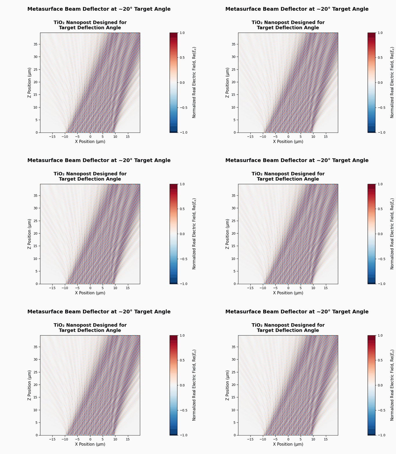
Diffraction-efficiency curves provide a quantitative comparison, but the field distributions make the physical differences across metasurface designs easier to interpret. For metasurfaces designed near the target angle, full-wave simulations show a relatively clean transmitted wavefront propagating in the intended direction. Off-design and low-index reference cases leave more power in the zero order and couple light into unwanted transmitted orders.
This is not simply a reduction in total transmission. It is a redistribution of power away from the desired +1 order. At the system level, that power can become stray light that shows up as unwanted background signal or ghost images.

The main point is not that every metasurface will outperform every conventional DOE. A metasurface that is not well matched to the target specification can perform poorly, and a well-designed DOE can perform extremely well. The relevant comparison is between structures that are each reasonably optimized for the same specification and with proper design assumptions (i.e., period is high enough to prevent aliasing, materials used are appropriate choices for metasurface performance, etc.)
Limitations of this Analysis
The DOE results here are intended to be indicative rather than absolute performance limits. While the efficiency estimates account for full-wave effects using rigorous coupled-wave analysis, the grating designs themselves utilize a scalar model that assumes that each region applies an independent phase delay and does not fully capture coupling between relief levels, vector diffraction, thin-film effects, or antireflective coatings. More sophisticated structures, including echelle gratings optimized for higher orders, continuous blazes, or otherwise rigorously optimized subwavelength multi-level gratings, may perform better than the binary staircase profiles considered here.
The metasurface results also do not represent an upper bound. They use relatively simple square-cross-section nanoposts rather than complex geometries, topology optimization, multilayer structures, or more sophisticated supercell designs. Those additional degrees of freedom can be especially valuable at large deflection angles.
The comparison should therefore be interpreted as two representative approaches under stated assumptions, not the best possible DOE against the best possible metasurface.
So, Which One Is Better?
At low diffraction angles, conventional multi-level DOEs can work very well. If the desired function is limited to spatial phase modulation, the choice may primarily come down to manufacturing, cost, and production volume. There may still be economic reasons to use a metasurface, particularly if it can be integrated into an existing semiconductor or nanoimprint process, but the intrinsic optical advantage may be limited.
At higher angles, the trade space changes. The phase period becomes smaller, the conventional relief profile becomes more difficult to sample, and scalar diffraction theory begins to lose validity. A metasurface designed specifically for the target wavelength, polarization, and angle can then provide substantially higher +1-order efficiency than a conventional DOE constrained to coarser features.
There is no universal angle at which one platform abruptly becomes superior. Instead, there is a gradual transition in which phase sampling, fabrication limits, material properties, and full-wave electromagnetic effects become increasingly important.
Neither “metasurfaces are always better” nor “binary optics are always better” is a useful conclusion. At modest phase gradients, the two platforms may produce similar results and economics may dominate the decision. At large phase gradients, the electromagnetic design matters, and comparisons based on an arbitrary material or a single metasurface geometry can can lead to misleading conclusions. At high phase gradients, the distinction between the platforms may become largely semantic. A multi-level grating optimized using full-vector methods could outperform a simple single-layer nanopost metasurface, but it also operates in the same subwavelength, vectorial regime that is commonly associated with metasurfaces. While some may disagree on the categorization, we would argue that this type of structure actually is a “metasurface”, given that the relevant feature scales are subwavelength and vector effects matter.
The beam deflectors considered here provide a simple way to isolate these effects, but the implications are unlikely to be limited to uniform gratings. More complex phase profiles can be interpreted locally as combinations of different phase gradients and deflection angles. A lens, for example, transitions from small deflection angles near its center to progressively larger angles toward its edge. This does not establish a universal performance result for every optical function, but it provides a plausible physical basis for expecting the same sampling, material, and full-wave effects to remain relevant in more complex devices.
References
Majumder, A., Doughty, J. A., Hayward, T. M., Smith, H. I., & Menon, R. (2025). Fresnel zone plate outperforms the metalens at high NA. Optics Express, 33(11), 23313-23321.
Menon, R., & Sensale-Rodriguez, B. (2023). Inconsistencies of metalens performance and comparison with conventional diffractive optics. Nature Photonics, 17(11), 923-924.
Arbabi, A., & Faraon, A. (2024). On” Inconsistencies of metalens performance and comparison with conventional diffractive optics”. arXiv preprint arXiv:2410.12559.
Engelberg, Jacob, and Uriel Levy. “The advantages of metalenses over diffractive lenses.” Nature communications 11.1 (2020): 1991.
Sacchi, L., Palmieri, A., Mishra, V., Park, J. S., Piccardo, M., & Capasso, F. (2025). Silica meta-optics: when high performance does not need a high index. Nano Letters, 25(50), 17448-17457.
Yang, J., & Fan, J. A. (2017). Topology-optimized metasurfaces: impact of initial geometric layout. Optics Letters, 42(16), 3161-3164.
Sell, D., Yang, J., Doshay, S., Yang, R., & Fan, J. A. (2017). Large-angle, multifunctional metagratings based on freeform multimode geometries. Nano letters, 17(6), 3752-3757.
Yang, J., & Fan, J. A. (2017). Analysis of material selection on dielectric metasurface performance. Optics express, 25(20), 23899-23909.
Bayati, E., Zhan, A., Colburn, S., Zhelyeznyakov, M. V., & Majumdar, A. (2019). Role of refractive index in metalens performance. Applied optics, 58(6), 1460-1466.